- News Category
- Industry News
- Product Information
- FAQ
- Customer Cases

What is PCI Express (PCIe)_ – How it Works?
Definition
PCIe, or Peripheral Component Interconnect Express, is a standard for connecting a computer's motherboard with peripherals such as graphics cards, sound cards, and solid-state drives. A PCIe card plugs into a corresponding slot on the motherboard, with types ranging from x1 to x16, indicating the number of data lanes available. More lanes mean higher data transfer rates, akin to more lanes on a highway enabling faster traffic flow. The standard is maintained by the Peripheral Component Interconnect Special Interest Group (PCI-SIG). For nearly 30 years, PCIe has been a key I/O connection, providing energy-efficient, high-bandwidth, and low-latency communication between computer components. PCIe is widely used in various applications ranging from handheld devices to high-performance computing and data centers, excelling in interoperability, capacity, and bandwidth. Its robust infrastructure also supports other protocols, such as Compute Express Link (CXL®), fully utilizing the software stack and platform connectivity capabilities of PCIe.
How Does PCI Express Work?
PCI Express (PCIe) operates as a serial connection, akin to a network rather than a traditional bus. Instead of a single bus managing data from various sources, PCIe employs a switch directing multiple point-to-point serial connections. Each device has its dedicated connection, eliminating the need for shared bandwidth as with conventional buses. A PCIe lane, crucial for communication between devices or the CPU, consists of two wires: one for incoming data and a second with double the bandwidth for outgoing data. These lanes ensure rapid bit transfer over electrical wires, with the number of lanes in a PCIe device denoted as xN, signifying its bandwidth capacity.
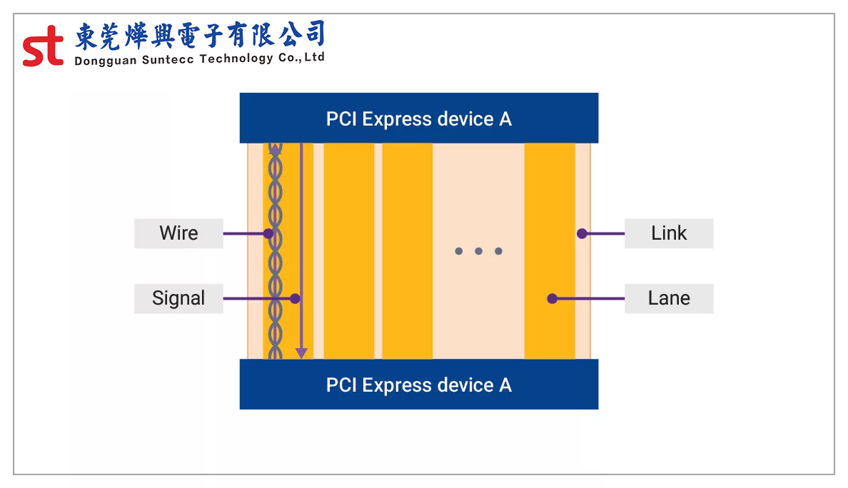
Figure 1: PCI Express Devices
PCIe incorporates high-speed serial communication, point-to-point connections, switch-based architecture, and a packetized protocol. The efficiency of PCIe heavily hinges on link negotiation and training, making the capturing and observation of dynamic link activities fundamental to its debugging. Analogous to the seven-layer OSI model in networking, PCIe operates on a layered architecture (Figure below).
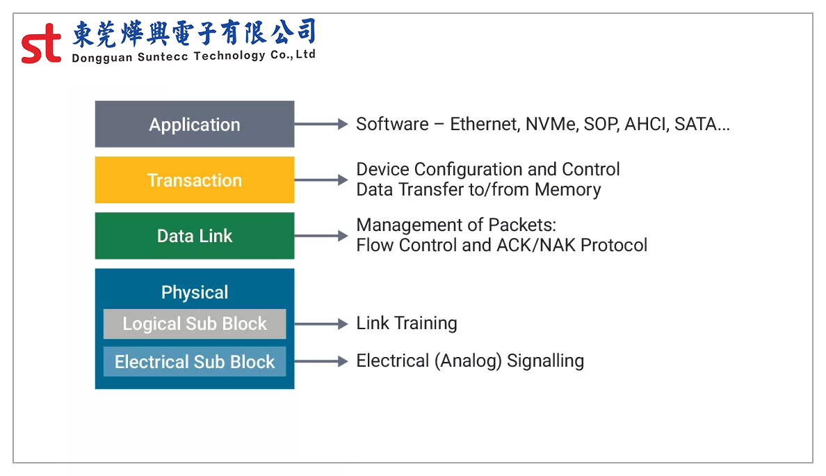
PCIe Architecture includes application, transaction, data link and physical layers.
PCIe Layered Architecture Breakdown
- Application Layer (Host Layer): This doesn't fall strictly within the PCIe specification. It encompasses protocols like Ethernet and NVMe as payload. PCIe primarily sets out the method for data transfer, without specifying payload content.
- Transaction Layer: Responsible for device configuration on the link. It facilitates memory transfers between host memory and the device, encompassing commands for memory read/write configurations. It also provides message and error reporting mechanisms.
- Data Link Layer: Manages data transfer between devices. Houses the flow control and acknowledgement protocols to ensure packet integrity. It also controls transitions to low power states, signaling the physical layer about power-saving intents.
- Physical Layer: Divided into two:
1. Electrical Sub-block: Contains the analog components essential for analog signaling.
2. Logical Sub-block: Dictates device communication using state machines and produces ordered data patterns and training sequences for link training.
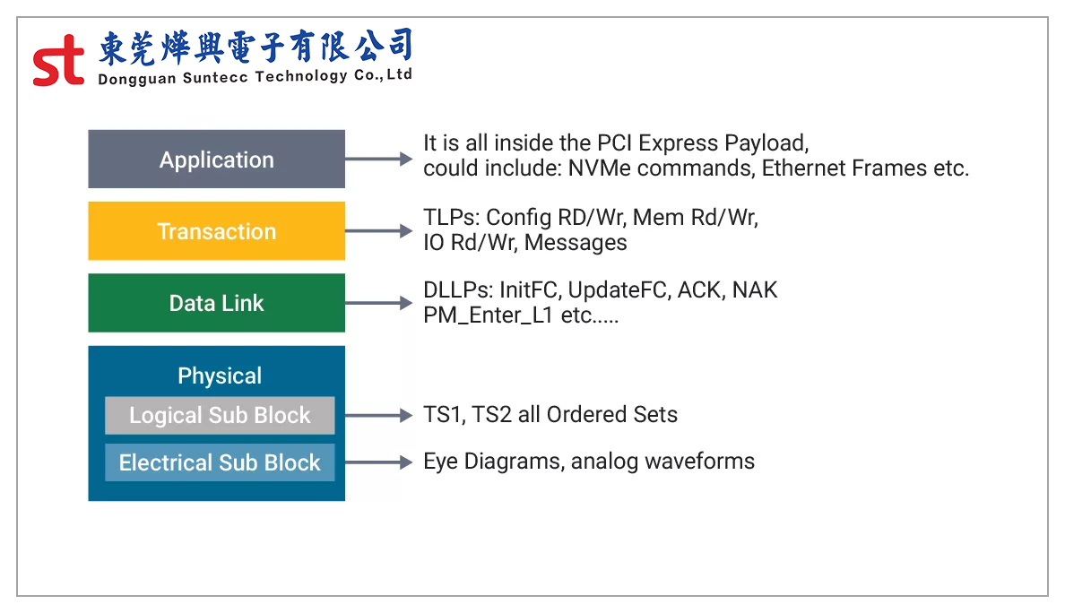
Typical Transactions at Each Layer of PCIe Operation
A PCIe link is established when two devices communicate. As shown in the figure below, both sides have a transmitter (TX) and a receiver (RX). The application layer facilitates data transfer between the root complex/host and the endpoint over this link. The corresponding device driver generates PCIe traffic, which traverses from the transaction layer to the datalink layer, then to the physical layer, and finally to the opposite side of the link.
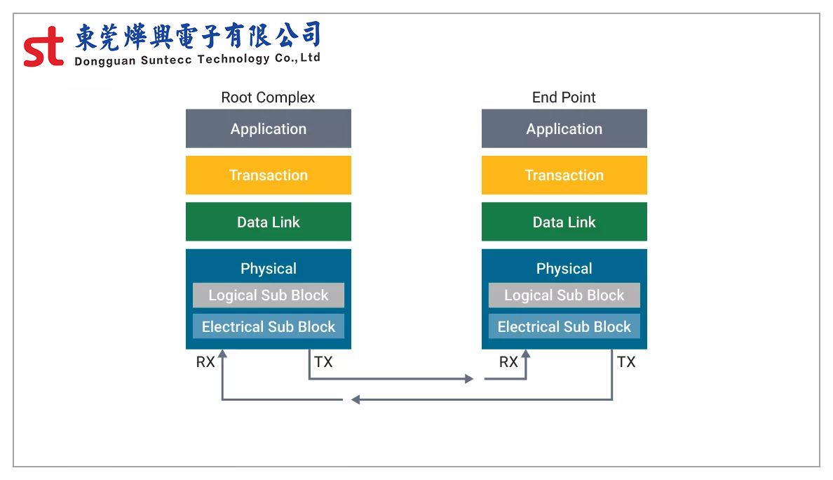
Anatomy of a PCIe Link
PAM-4 Signaling vs. NRZ Signaling
Hyperscale data center service providers must allow faster interfaces, because of this PCIe transitioned from PCIe 5.0 using NRZ to PCIe 6.0 using PAM-4. Using the PAM-4 signaling is critical because Non-Return to Zero (NRZ) signaling is no longer able to support data rates beyond 32G for lossy channels beyond just few decibels (dB) of insertion loss. For further detail, see this article on PAM-4 multi-level signaling and its trade-offs and benefits vs. NRZ.
Compared to NRZ’s two voltage levels, PAM-4 has four voltage levels that result in 12 distinct signal transitions, (six rise & six fall times) creating three district eye openings, as shown in the figure below. Each eye height is 1/3 of an NRZ eye height, causing the PAM-4 signal-to-noise ratio (SNR) to degrade by over 9.5 dB, which impacts the signal quality and introduces additional constraints in high-speed signaling. The 33% smaller vertical eye opening reduces the signal’s tolerance to crosstalk and reflection in PAM-4 resulting in a higher bit error rate.
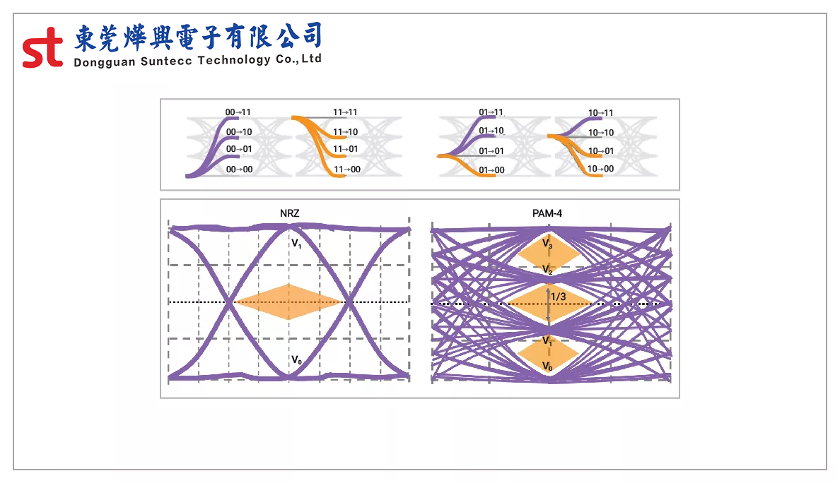
NRZ vs. PAM4 Signal Transitions and Eye Diagram Openings
What is New with PCI Express 7.0 (PCIe 7.0)?
PCI-SIG released PCIe 7.0 technology in 2022 and plans to release the full specification in 2025. This development aims to meet the huge bandwidth demands of data-intensive applications and markets, including artificial intelligence/machine learning (AI/ML), 1.6T/800G Ethernet networks, high-performance computing (HPC), and quantum computing in high-performance computing data centers. PCIe 7.0 will provide low-latency, low-power, and reliable connections between accelerators, processors, network interface cards (NICs), and other components, ensuring efficient connectivity in high-performance computing environments.
- Higher Bandwidth: PCIe 7.0 offers twice the bandwidth of PCIe 6.0, with bidirectional transfer speeds up to 512 GB/s, featuring 16 channels at 128 GT/s. This enhanced bandwidth is crucial for rapidly and efficiently processing large amounts of data, which is essential for AI and HPC applications.
- Low Latency: By increasing the signal rate, PCIe 7.0 reduces latency, which is crucial for real-time processing and response capabilities of AI algorithms and high-speed data processing in HPC.
- Compatibility and Scalability: PCIe 7.0 maintains backward compatibility with previous generations of PCIe, ensuring interoperability with existing hardware and providing scalability for future upgrades. This is crucial for seamlessly integrating new technologies into existing AI and HPC infrastructures.
- Energy Efficiency: Despite performance improvements, PCIe 7.0 aims to maintain or enhance energy efficiency, which is critical for reducing overall operational costs and environmental impact in data centers and large computing facilities.
- Advanced Features: PCIe 7.0 introduces new features and optimizations that further enhance its practicality in demanding applications, including improved channel margin features, enhanced error detection and reporting mechanisms, and support for emerging technologies such as CXL.
- Channel Reach and Signal Integrity Considerations: The targeted channel reach for PCIe 7.0 remains consistent with PCIe 6.0, employing 4 inches - 14 inches system cabling in a single connection topology and 2 inches - 4 inches AIC cabling, with pad-to-pad channel loss up to -36dB. To minimize insertion loss and reflections in the root complex reference package, connector insertion loss, return loss, PCB loss, and via insertion and return loss are minimized by reducing crosstalk.
Why is PCI Express Compliance Important?
With the rise of technological advancements, there's a growing demand for faster CPUs, quicker memory solutions, and advanced consumer devices. This amplifies the need for enhanced system interconnectivity and broadened bandwidth. Standards like PCIe serve this very purpose, catering to diverse sectors from data centers and AI/machine learning to cloud solutions.
Within chip design, compatibility across products in the market remains a top priority. PCI-SIG Compliance Testing plays a pivotal role in ensuring this. Manufacturers submit their products to PCI-SIG Compliance Workshops to verify their adherence to crucial PCIe specifications and, crucially, to ensure seamless integration with other ecosystem products, irrespective of the vendor. While companies can undertake in-house tests for cross-vendor compatibility, achieving PCIe compliance offers a more robust validation of a product's interoperability, endorsed by industry frontrunners. Thus, with this compliance seal, developers can proceed with their chip designs, confident in their product's capability to integrate seamlessly with others in the marketplace.
What Solutions Does Suntecc Offer?
Dongguan Suntecc Technology Co., Ltd. is a branch of TC&C Electronics Co.,Ltd, as a leading high-speed cable provider, Suntecc continues to empower the entire PCIe ecosystem. High-speed cable products include PCIe 6.0 cables, PCIe 5.0 cables, PCIe 4.0 cables, MCIO 4X cables, MCIO 8X cables, MCIO 16X cables, SFF 8654 4X cables, SFF 8654 8X cables, Oculink (8611) cables, SFF 8639 (U.2/U.3) cables, Mini-SAS-HD (8643) cables, 12VHPWR PCIe 5.0 power cables, etc. Yexing Electronics has over 20 years of experience in the PCIe field and has completed over 3,000 designs in collaboration with global leading companies. The solutions are designed to support PCIe 7.0 128 GT/s (Gen7), PCIe 6.0 64GT/s (Gen6), PCIe 5.0 32GT/s (Gen5), PCIe 4.0 16GT/s (Gen4), 3.1 8GT/s (Gen3), 2.1 5GT/s (Gen2), and 1.1 2.5GT/s (Gen1).
Suntecc offer PCIe high-speed cable solutions that provide high-throughput, low-latency, and efficient external connections for SoCs in mobile networks, storage, cloud computing, artificial intelligence, and automotive applications. We have conducted extensive interoperability testing with third-party products and implemented rigorous quality measures, along with a professional technical support team, enabling designers to accelerate product time-to-market and reduce integration risks.
2025-08-28
